As the cloud revolution whisked enterprises off their feet, they found themselves treading robust, and distributed infrastructures. This cloud, unlike their office datacenters, ran out of server farms in remote places, and had a shared, multi-tenant occupancy. Now they are working their way up to the next level – cloud-native.
At last week’s Cloud Field Day event, AMD tapped into the discussion of cloud nativity. Presenter, Robert W Hormuth, CVP of Architecture and Strategy at AMD, took the audience on a journey into the evolution of workloads, and the potential of cloud-native chip design.
From Local computing to Cloud Native
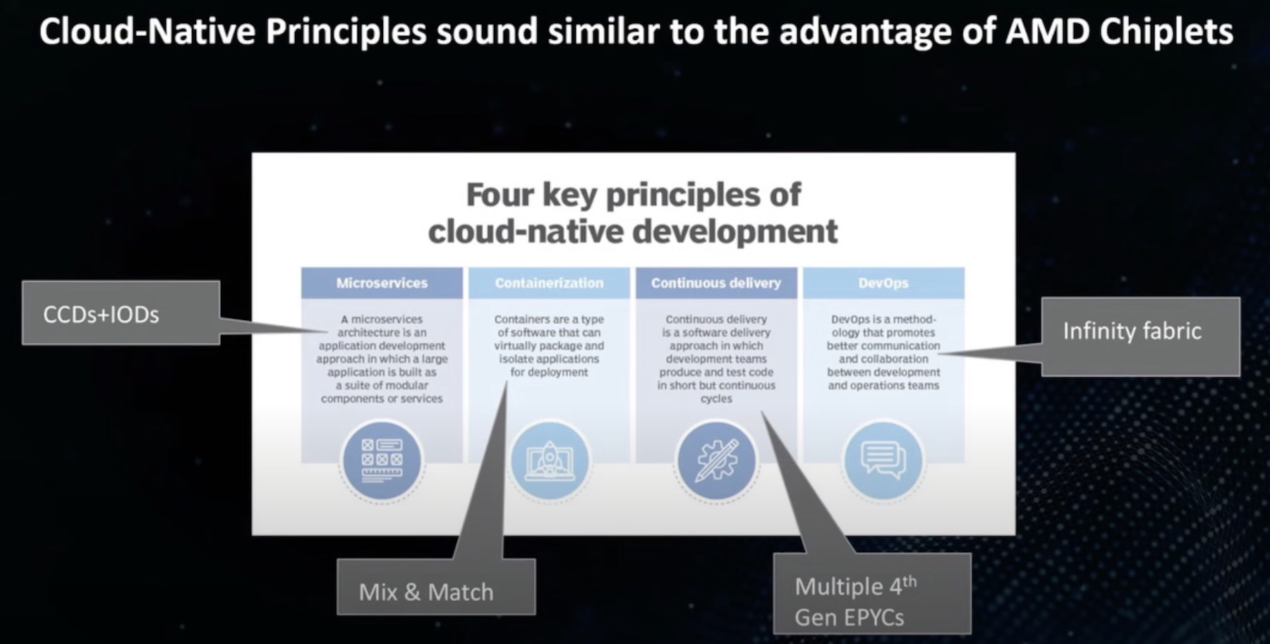
To understand cloud-native, it is important to skim through the timeline of cloud computing. At the basic level, four core tenets drive cloud-native – microservices, containerization, continuous delivery, and DevOps. Back in the day, applications were built and deployed from local datacenters. These datacenters, depending on their size, were located in the backyard, basement or somewhere on premises.
This generation of applications were written in monolithic blocks of code. Storage, network and compute were available in limited quantities, and the infrastructure was controlled end to end by the owners themselves.
Then the world stepped into the era of virtualization. Virtual machines or VMs called for modular and lightweight designs. Thus containers were born. Applications that used to be big and blocky were broken down into microservices and containerized. This made each service a tiny application, running independently inside the container while sharing the operating system with others. Each containerized application could be granularly upgraded or modified without affecting the others.
“The virtual world started to change the landscape. Now we have tens of applications, maybe hundreds, depending on your scale of enterprise, and where your comfort level is. There’s a lot of stark differences between those kinds of applications,” he highlighted.
This transition triggered a need for change in the hardware. “It drove a different kind of architecture at the SoC (system on a chip) level. It drove higher memory capacity because now they’re packing in a lot of these large monolithic applications into larger VMs,” said Hormuth.
Most legacy applications were ported over from monolithic to virtualization, a process that is as slow as it is back-breaking. But as enterprises get to containers, and the more recent, function-as-a-service (FaaS), things start to get harder. They demand more and more infrastructure services and CPU resources.
Function-as-a-service came to be offered as a way to help customers respond to events without navigating the infrastructural complexities. Offered as a set of features, the FaaS applications are short-lived and come with a range of system-level overheads.
Cloud-Native Workloads Need Cloud-Native Processing
A developers’ dream-come-true, on the downside, microservices posed a new challenge. It gave them an enormous population of containers to manage and look after. So, Kubernetes was developed to orchestrate these containers in an orderly fashion. But there was still the matter of provisioning physical resources on demand.
Enter cloud providers. These companies built mega infrastructures, large enough to rent out resources on demand to smaller businesses. Colossal datacenters spanning acres of land mushroomed across continents swapping out infrastructural overheads with ready cloud-managed services. These services ensured that the applications continually received physical resources whenever required.
With the rise of FaaS applications, companies are more inclined to take advantage of these cloud-based backend services. To support the evolving workloads, the hardware architecture too has to change. High-capacity, multi-core CPUs have come in to handle computationally intensive processing. Hyperscalers absorb these into their infrastructures, making the latest and greatest technologies available at the customers’ fingertips.
These CPUs sport features like simultaneous multi-threading (SMT) that enables physical cores to be divided into logical threads for simultaneous execution of instruction sequences.
Ceding application hosting to these providers helps overcome a lot of the limitations of the local datacenters, and provides unforeseen resilience and availability. But it has tradeoffs. Despite the state-of-the-art technologies, a multi-tenant environment can have performance predictability issues, nonlinear scalability and cost escalation which heavily impact the cloud service provider (CSP) business model.
When applications with competing resource requirements run in the same environment, for example, sharing two simultaneous threads of one core, the heavy resource requirements of one application can starve the other out, causing it to slow down and suffer a QoS drop. Insiders call it the “noisy neighbor” issue.
Besides, security is tricky in a shared infrastructure. SMT threads typically provide low isolation between customers, leaving data vulnerable to side-channel attacks.
One way to get around the problem is to assign dedicated hardware to individual customers which keeps them from sharing their resources with others. This may make it easier to meet service level agreement (SLA), but it heavily undercuts the cloud economics. The cloud business model rests on economies of scale, meaning the more the hosted users per server, more the profit and greater the customers’ savings.
DPU mitigates a lot of these problems. DPU or Data processing unit is an SoC that combines three key elements – a multi-core CPU, a high-performance network interface, and acceleration engines. Designed to move data around and process it, DPU offloads the networking and communication workloads from the CPU by tackling data-centric workloads on its own.
The fully-programmable AMD Pensando DPU opened doors to hardware composability and heterogenous computing. It optimized performance by freeing up CPU resources, and added a new layer of security at cloud scale.
Cloud-Native and AMD
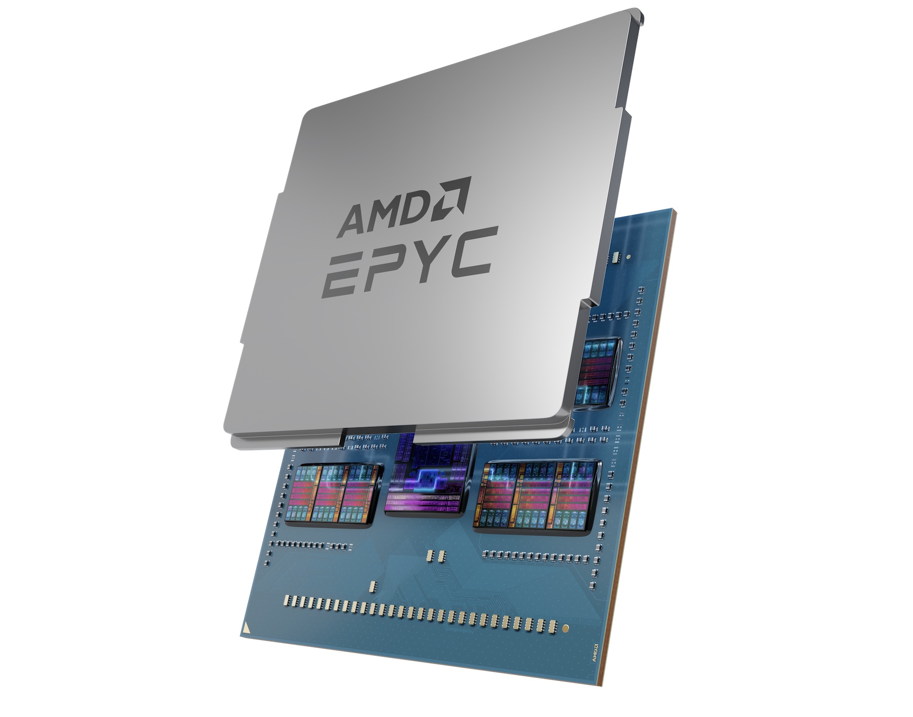
AMD knew that’s what’s required is a chip-level reformation. In 2019, AMD introduced the industry’s first chiplet-based technology which held great promises in terms of flexibility, cost savings and scalability. It accommodates different process nodes and IO together unlocking significantly higher performance and capabilities. The approach flipped traditional chip architecture on its head opening new possibilities for companies looking to go cloud-native.
“To us, cloud native is an approach to application development. It’s not a thing a place or a cloud. It’s an approach to developing applications, and the speed of development. It’s about mixing DevOps and microservices and modern deployment tools, and managing that scale so that when you need more resources, you can spin them up. When you don’t need them, you can spin it down but still get that application scalability,” said Hormuth.
Traditionally chips are built on a single die and made from scratch. The chiplet architecture uses smaller pieces, referred to as “chiplets”, which the design brings together into a new server chip. The package architecture allows granular control and targeted customization, enabling the manufacturer to flexibly configure based on the specific power, performance and cost demands of a product.
AMD’s state-of-the-art chiplet architecture aligns well with the cloud-native principles noted earlier. Already known for its High Bandwidth Memory (HBM) technology that provides the best memory bandwidth in small form factor in the GPU market, AMD broke barriers by introducing the multi-chip module (MCM) packaging in 2017.
The 3D architecture is optimized to provide highest bandwidth within the lowest silicon area possible. The design which relies on die-to-die interconnect, uses copper-to-copper hybrid bonding. In the architecture, dies are stacked and connected via copper-to-copper bonding giving it its 3D form and enabling extreme performance at almost no power or signal penalties. This ensures a tighter and denser integration between IP blocks, delivering 200x better interconnect density compared to AMD’s 2D chiplets.
Watch the full presentation from the recent Cloud Field Day event to learn how AMD is leading the cloud-native revolution with Pensando DPU and the EPYC portfolio.